- 您现在的位置:买卖IC网 > Sheet目录477 > MICRF221AYQS TR (Micrel Inc)IC RF RECEIVER QWIKRADIO 16-QSOP
Micrel Inc.
MICRF221
REFOSC (MHz)
13.54856
14.27643
14.29983
Carrier (MHz)
868.35
915.0
916.5
HIB Part Number
SA-13.548560-F-10-H-30-30-X
SA-14.276430-F-10-H-30-30-X
SA-14.299830-F-10-H-30-30-X
Abracon Part Number
ABLS-13.54860MHz-10-J4Y
ABLS-14.276430MHz-10-J4Y
ABLS-14.299830MHz-10-J4Y
Table 4. Crystal Frequency and Vendors Part Number
data packets and if the data pattern has or does not
Demodulation Bandwidth Calculation
JP1 and JP2 are used to select the bandwidth for the
have a preamble. See Figure 9 for an example of a
data profile.
demodulator. To set the bandwidth correctly, it is
necessary to know the shortest pulse width of the
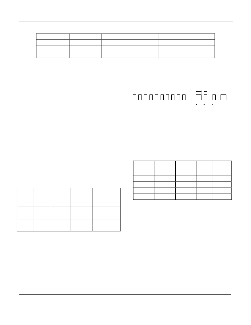
PREAMBLE
PW1 PW2
encoded data sent in the transmitter. As shown in the
example of the data profile in the Figure 9 below, PW2
is shorter than PW1, so PW2 should be used for the
demodulator bandwidth calculation which is found by
1
2
3
4
5
6
7
8
9
HEADER
10
t1 t2
PW2 = NARROWEST PULSE WIDTH
calculating 0.65/shortest pulse width. After this value
is found, the setting should be done according to
Table 5.
For example, if the pulse period is 100μsec, 50% duty
cycle, the pulse width will be 50μsec:
(PW = (100μsec × 50%) / 100)
So, a bandwidth of 13kHz would be necessary (0.65 /
t1 & t2 = DATA PERIOD
Figure 9. Example of a Data Profile
For best results C4 and C6 should be optimized for
the data pattern used. As the baud rate increases, the
capacitor values decrease. Table 6 shows suggested
values for Manchester Encoded data at a 50% duty
cycle.
50μsec). However, if this data stream had a pulse
period with 20% duty cycle, the bandwidth required
would be 32.5kHz (0.65 / 20μsec), which exceeds the
maximum bandwidth of the demodulator circuit. If you
try to exceed the maximum bandwidth, the pulse will
appear stretched or wider.
SEL0
JP1
Short
Open
SEL1
JP2
Short
Short
Demod.
BW
(hertz)
1712
3425
C TH
100nF
47nF
C AGC
4.7μF
2.2μF
SEL0
SEL1
Demod.
Shortest
Maximum
Short
Open
6850
22nF
1μF
JP1,
D3
Short
Open
Short
JP2,
D4
Short
Short
Open
BW
(hertz)
1712
3425
6850
Pulse
(μsec)
380
190
95
baud rate for
50% Duty
Cycle (hertz)
1316
2632
5264
Open Open 13700 10nF 0.47μF
Table 6. Suggested C6 (C TH ) and C4 (C AGC ) Values
JP4 (pins 5 and 6) is a jumper used to configure the
digital squelch function. When pin 6 (SQ) is held high
Open
Open 13700 47 10528
Table 5. JP1 and JP2 setting, 915 MHz
jumpered-to-V DD ), there is no squelch applied to the
digital circuits and pin 10 (DO, data out) has a hash
signal. When pin 6 (SQ) is low, the DO pin activity is
This device is capable of higher baud rates when the
serial bit D16 is programmed high. More detail is
provided on the following pages.
C TH and C AGC Selection
Capacitors C6 (C TH ) and C4 (C AGC ) provide time base
reference for the data pattern received. These
capacitors are selected according to the data profile,
pulse duty cycle, dead time between two received
considerably reduced. It will have more or less activity
than is shown in Figure 11 depending upon the
outside band noise. The penalty for using squelch is a
delay in getting a good signal at the DO pin, that is, it
takes longer for the data to show. The delay is
dependent upon many factors such as RF signal
intensity, data profile, data rate, C TH and C AGC
capacitor values and outside band noise. See Figures
10 and Figure 11.
October 2008
15
M9999-100108
(408) 955-1690
发布紧急采购,3分钟左右您将得到回复。
相关PDF资料
MICRF300YC6 TR
IC AMP 100/1000MHZ LN SC70-6
MICRF500BLQTR
TXRX UHF 700-1100MHZ 44-LQFP
MICRF501BLQ TR
TXRX SGL 300-600MHZ 44-LQFP
MICRF505DEV1
KIT DEV RADIOWIRE 850-950MHZ
MICRF506DEV1
EVAL BOARD EXPERIMENTAL MICRF506
MICRF507YML TR
TXRX FSK LOW PWR W/AMP 32MLF
MICRF600DEV1
KIT DEV RADIOWIRE 902-928MHZ
MK01-C
SENSOR REED SPST-NO SMD
相关代理商/技术参数
MICRF229YQS-T5
功能描述:- RF Receiver ISM 433.92MHz -112dBm 20kbps On-Board, Trace 16-QSOP 制造商:microchip technology 系列:- 包装:剪切带(CT) 零件状态:停产 频率:433.92MHz 灵敏度:-112dBm 数据速率(最大值):20kbps 调制或协议:ISM 应用:通用 电流 - 接收:6mA 数据接口:- 存储容量:- 天线连接器:板载,跟踪 特性:- 电压 - 电源:3.5 V ~ 5.5 V 工作温度:-40°C ~ 105°C 封装/外壳:16-LSSOP(0.154",3.90mm 宽) 供应商器件封装:16-QSOP 标准包装:1
MICRF229YQS-TR
功能描述:- RF Receiver ISM 433.92MHz -112dBm 20kbps On-Board, Trace 16-QSOP 制造商:microchip technology 系列:- 包装:剪切带(CT) 零件状态:停产 频率:433.92MHz 灵敏度:-112dBm 数据速率(最大值):20kbps 调制或协议:ISM 应用:通用 电流 - 接收:6mA 数据接口:- 存储容量:- 天线连接器:板载,跟踪 特性:- 电压 - 电源:3.5 V ~ 5.5 V 工作温度:-40°C ~ 105°C 封装/外壳:16-LSSOP(0.154",3.90mm 宽) 供应商器件封装:16-QSOP 标准包装:1
MICRF230YQS-T5
功能描述:- RF Receiver ISM 433.92MHz -112dBm 20kbps On-Board, Trace 16-QSOP 制造商:microchip technology 系列:- 包装:剪切带(CT) 零件状态:停产 频率:433.92MHz 灵敏度:-112dBm 数据速率(最大值):20kbps 调制或协议:ISM 应用:通用 电流 - 接收:6mA 数据接口:- 存储容量:- 天线连接器:板载,跟踪 特性:- 电压 - 电源:3.5 V ~ 5.5 V 工作温度:-40°C ~ 105°C 封装/外壳:16-LSSOP(0.154",3.90mm 宽) 供应商器件封装:16-QSOP 标准包装:1
MICRF230YQS-TR
功能描述:- RF Receiver ISM 433.92MHz -112dBm 20kbps On-Board, Trace 16-QSOP 制造商:microchip technology 系列:- 包装:剪切带(CT) 零件状态:有效 频率:433.92MHz 灵敏度:-112dBm 数据速率(最大值):20kbps 调制或协议:ISM 应用:通用 电流 - 接收:6mA 数据接口:- 存储容量:- 天线连接器:板载,跟踪 特性:- 电压 - 电源:3.5 V ~ 5.5 V 工作温度:-40°C ~ 105°C 封装/外壳:16-LSSOP(0.154",3.90mm 宽) 供应商器件封装:16-QSOP 标准包装:1
MICRF300-315 EV
功能描述:EVAL BOARD FOR MICRF300 制造商:microchip technology 系列:- 零件状态:无货 类型:放大器 频率:315MHz 配套使用产品/相关产品:MICRF300 所含物品:板 标准包装:1
MICRF300-433 EV
功能描述:EVAL BOARD FOR MICRF300 制造商:microchip technology 系列:- 零件状态:无货 类型:放大器 频率:433.92MHz 配套使用产品/相关产品:MICRF300 所含物品:板 标准包装:1
MICRF300-915 EV
功能描述:EVAL BOARD FOR MICRF300 制造商:microchip technology 系列:- 零件状态:无货 类型:放大器 频率:915MHz 配套使用产品/相关产品:MICRF300 所含物品:板 标准包装:1
MICRF300YC6
制造商:MICREL 制造商全称:Micrel Semiconductor 功能描述:100MHz to 1000MHz, 1.8 to 3.6V, Low-Noise Amplifier with Shutdown
